


Aug 27, 2025
Type-II Superlattices (T2SL) are a class of engineered semiconductor materials that have emerged as a powerful alternative to traditional infrared (IR) detector technologies. Developed primarily to enhance infrared imaging performance while reducing cost and complexity, T2SL structures offer tunable optoelectronic properties and are at the forefront of next-generation sensing technologies.
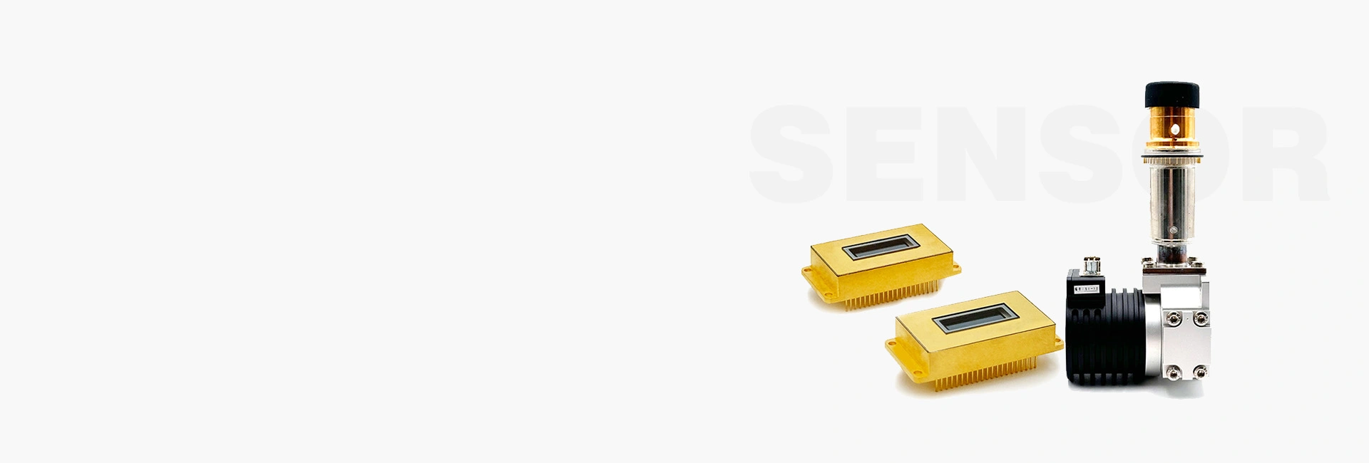
At its core, a superlattice is a periodic structure made of alternating layers of two or more different semiconductor materials. In Type-II Superlattices, the conduction band minimum and valence band maximum are located in different layers, leading to a spatial separation of electrons and holes. This unique band alignment and carrier separation mechanism make Type-II superlattices particularly attractive for advanced infrared CMOS image sensor technologies, where precise control of infrared absorption, carrier dynamics, and noise performance is critical for high-sensitivity imaging applications.
Common T2SL materials include combinations such as InAs/GaSb and InAs/InAsSb. These materials are grown using molecular beam epitaxy (MBE) with nanometer-scale precision, allowing designers to control the energy bandgap and optimize the material’s response to specific infrared wavelengths. This band engineering is one of the most powerful aspects of T2SL technology, as it enables detection across multiple infrared bands, from mid-wave IR (MWIR) to long-wave IR (LWIR).
T2SL-based infrared detectors offer several distinct advantages over traditional materials like mercury cadmium telluride (HgCdTe). One of the most significant benefits is the lower dark current, which directly translates to better signal-to-noise ratios in imaging applications. This makes T2SL detectors highly suitable for low-light or high-sensitivity environments.
Moreover, T2SL materials are inherently more compatible with standard III-V semiconductor processing techniques, allowing for better scalability, uniformity, and integration with other optoelectronic devices. Their tunable bandgap and improved temperature stability also make them highly adaptable for a wide range of applications.
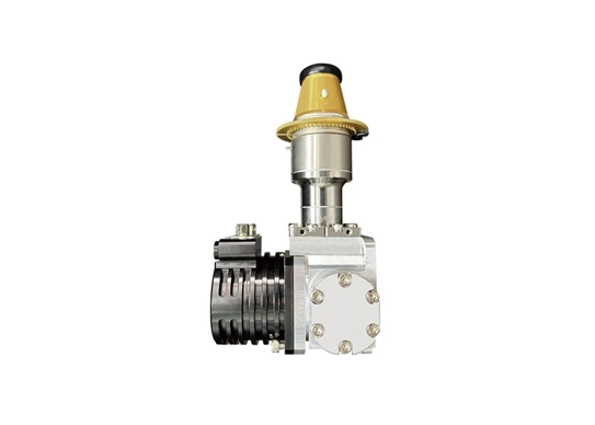
The versatility of T2SL has led to its adoption in various high-performance and mission-critical applications. In the defense and aerospace sectors, T2SL detectors are used in advanced thermal imaging systems for surveillance, targeting, and navigation. Their ability to function across multiple infrared bands is particularly valuable in environments where visibility is limited or conditions are extreme.
Beyond military use, T2SL detectors are also being applied in environmental monitoring, gas detection, and space-based telescopes. Industrial applications include non-destructive testing, thermal imaging for equipment maintenance, and scientific instrumentation that requires precise infrared sensitivity.
While T2SL technology holds great promise, several challenges remain. One of the primary hurdles is the complexity of material growth and interface control. The performance of a T2SL detector is highly sensitive to the quality of the interfaces between layers, and any lattice mismatch can lead to defects that degrade performance.
Additionally, noise characteristics and thermal management remain active areas of research. Achieving consistent detector performance at higher operating temperatures is a key goal for reducing cooling requirements and enabling more compact systems.
Ongoing developments focus on improving material quality, extending detection ranges (including very long-wave infrared, VLWIR), and optimizing integration with readout circuits. As research advances, T2SL is expected to continue replacing older infrared detector technologies in both commercial and government sectors.
1. What is a Type-II Superlattice (T2SL)?
A Type-II Superlattice (T2SL) is an engineered semiconductor structure made of alternating layers of different materials, where the conduction band minimum and valence band maximum are in separate layers. This unique band alignment enables superior control of bandgap and carrier separation for advanced infrared detection.
2. How does T2SL technology compare to traditional infrared detector materials?
T2SL infrared detectors offer several advantages over traditional materials like HgCdTe, including lower dark current, improved signal-to-noise ratio, scalable fabrication, and tunable detection range. These features make T2SL a strong candidate for next-generation high-performance infrared imaging, including integration with infrared CMOS image sensor systems.
3. What materials are commonly used in T2SL structures?
Common combinations include InAs/GaSb and InAs/InAsSb, which are grown with high precision using molecular beam epitaxy (MBE). Engineering the layer thicknesses allows designers to tailor the bandgap for specific infrared wavelength ranges.
4. What infrared wavelength ranges can T2SL detectors cover?
T2SL detectors can be engineered to detect across multiple infrared bands, including mid-wave IR (MWIR) and long-wave IR (LWIR). Their tunable bandgap enables applications from about 3 µm up to beyond 10 µm depending on the material design.
5. What challenges do T2SL detectors face?
Challenges include the complexity of precise material growth, managing interface quality, and optimizing detector performance at higher operating temperatures to reduce cooling requirements.
6. Can T2SL detectors be integrated with CMOS technology?
Yes — T2SL materials can be engineered and optimized for integration with readout circuits and infrared CMOS image sensor architectures, enabling compact, high-performance infrared imaging devices for diverse applications.
